🎯 Key Points
- Conductor: bands overlap; Insulator: large gap (>3eV); Semiconductor: small gap (Si=1.1eV, Ge=0.7eV)
- n-type: doped with pentavalent (P, As) — extra electrons are MAJORITY carriers; p-type: doped with trivalent (B, Al) — holes are MAJORITY carriers
- p-n junction: depletion region forms by diffusion; built-in field points n→p; Forward bias REDUCES barrier (current flows); Reverse bias INCREASES barrier (blocks current)
- Zener diode is specifically used in REVERSE breakdown for voltage regulation — unlike a normal diode which is meant to operate forward
- CE (common-emitter) is the most common transistor amplifier configuration due to its combination of decent current AND voltage gain
Band Theory
Conductors have overlapping bands, semiconductors have a small energy gap that can be bridged by heat or doping, and insulators have a large gap that blocks conduction.
- Conductor: overlapping or partially filled bands
- Insulator: large band gap (> 3 eV)
- Semiconductor: small band gap (Si: 1.1 eV, Ge: 0.7 eV)
- Intrinsic semiconductor: pure; equal holes and electrons
Doping
- n-type: doped with pentavalent (P, As, Sb); extra electrons are majority carriers
- p-type: doped with trivalent (B, Al, In); holes are majority carriers
p-n Junction
At the p-n junction, diffusion of carriers creates a depletion region depleted of free charges, with a built-in electric field pointing from the n-side to the p-side.
- Depletion layer: region of no free charge carriers near junction
- Forward bias: reduces barrier, allows current flow
- Reverse bias: increases barrier, blocks current (tiny reverse saturation current)
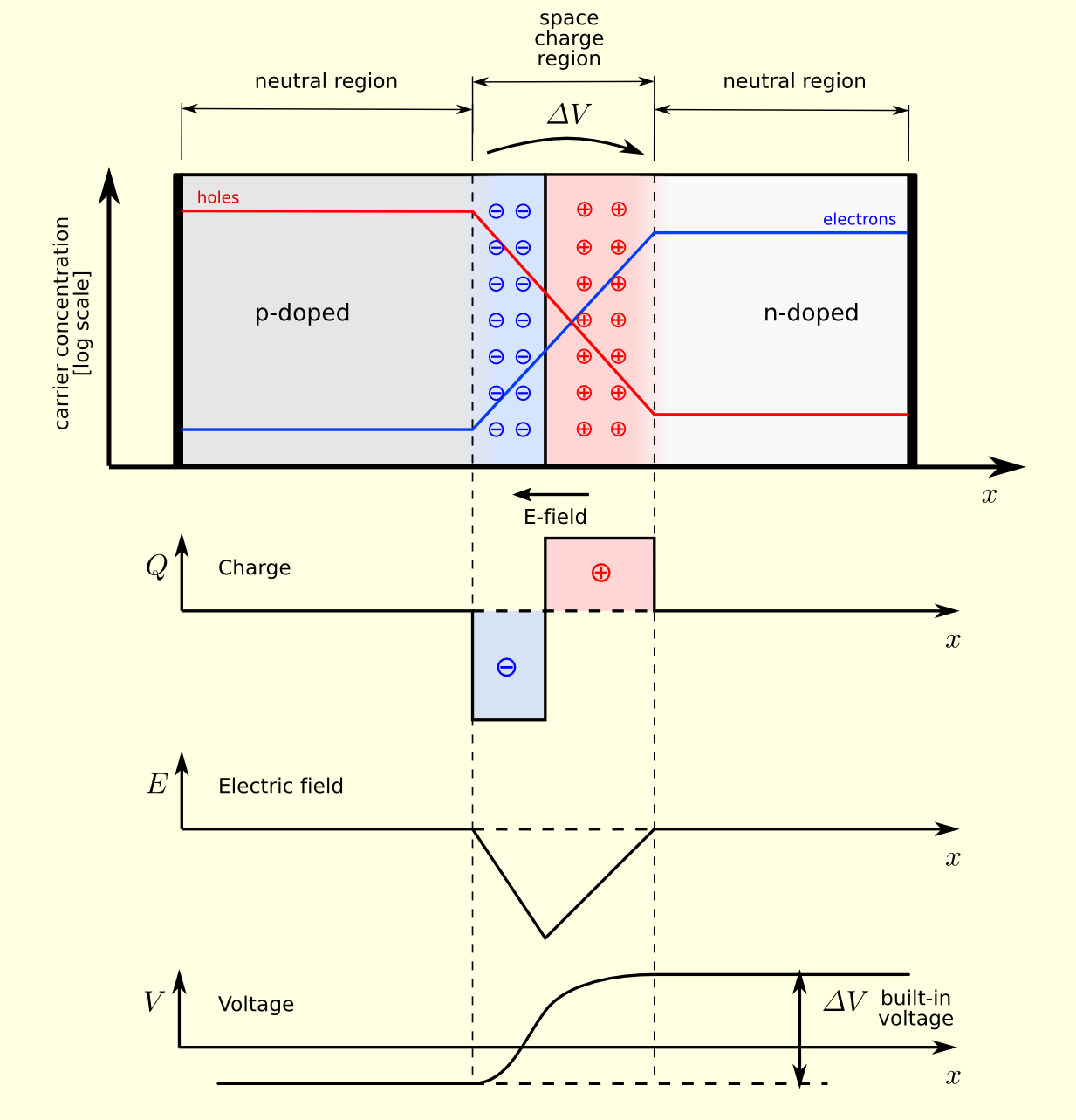
p-n junction in equilibrium: diffusion leaves a depletion (space-charge) region of fixed ions, setting up an internal field and a built-in potential barrier. Image: TheNoise, CC BY-SA 3.0, via Wikimedia Commons.
Devices
- Rectifier diode: converts AC to DC (half-wave and full-wave)
- Zener diode: voltage regulation (operates in reverse breakdown)
- LED: emits light when forward biased (direct band gap semiconductors)
- Photodiode: reverse biased; generates current when light absorbed
- BJT transistor: CB, CE, CC configurations; CE most common amplifier
- Logic gates: AND, OR, NOT, NAND, NOR, XOR
Intrinsic and Extrinsic Semiconductors
- Intrinsic: a pure semiconductor (Si, Ge) where thermally generated electrons and holes are equal in number (n_e = n_h = n_i); conductivity is very low and rises with temperature
- Extrinsic: conductivity greatly increased by adding a controlled impurity (doping), giving one type of carrier in excess
- n-type: pentavalent dopant (P, As, Sb) donates a free electron; electrons are majority, holes minority (n_e ≫ n_h)
- p-type: trivalent dopant (B, Al, In) creates a hole; holes are majority, electrons minority (n_h ≫ n_e)
- In any doped semiconductor the mass-action law holds: n_e·n_h = n_i², and the crystal stays electrically neutral overall
Junction Diode I-V Characteristics
- Forward bias (p to +, n to −): current stays tiny until the applied voltage exceeds the knee/threshold voltage (~0.7 V for Si, ~0.3 V for Ge), then rises sharply — the diode conducts
- Reverse bias: only a very small, nearly constant reverse saturation current flows (due to minority carriers)
- At a large reverse voltage the diode undergoes breakdown and reverse current increases abruptly
- The diode is a non-ohmic device: its resistance is low in forward bias and very high in reverse bias, making it act as a one-way valve for current
Rectifiers (AC to DC)
- Half-wave rectifier: a single diode conducts during only one half of each AC cycle, so the output is a pulsating DC present for half the time — low efficiency
- Full-wave rectifier: uses a centre-tapped transformer with two diodes (or a bridge of four diodes) so both halves of the AC cycle drive current the same way through the load — smoother, higher output
- The output ripple is reduced using a filter (capacitor) to give steadier DC
- Rectification is the first stage of almost every DC power supply that runs from the mains
Special Purpose Diodes
- Zener diode: heavily doped, operated in reverse breakdown at a fixed Zener voltage; it holds the voltage constant across a load, acting as a voltage regulator
- LED: forward-biased diode that emits light when electrons and holes recombine; photon energy ≈ band gap, so the colour depends on the semiconductor
- Photodiode: reverse-biased; incident light generates electron-hole pairs, so the reverse current increases with light intensity (used as a light detector)
- Solar cell: an unbiased junction that directly converts light into electrical energy (photovoltaic effect), generating a voltage across the junction when illuminated
Logic Gates and Truth Tables
- OR: output 1 if any input is 1 (A + B). Inputs 00,01,10,11 give outputs 0,1,1,1
- AND: output 1 only if all inputs are 1 (A·B). Inputs 00,01,10,11 give outputs 0,0,0,1
- NOT: single input inverter; output is the opposite of the input (input 0 gives 1, input 1 gives 0)
- NAND (AND then NOT): outputs for 00,01,10,11 are 1,1,1,0
- NOR (OR then NOT): outputs for 00,01,10,11 are 1,0,0,0
- NAND and NOR are universal gates — any logic circuit can be built using only NAND gates or only NOR gates
🚀 JEE Advanced Edge
Transistor as an amplifier — current/voltage gain: Current gain β=ΔI_C/ΔI_B (typically 50-200 for a BJT); voltage gain = β × (R_C/R_in). A small base current change controls a much larger collector current change, which is the basis of all transistor amplification.
NAND/NOR as universal gates: Any logic function (AND, OR, NOT, XOR, etc.) can be built using ONLY NAND gates (or only NOR gates) — this universality is why NAND/NOR are the actual building blocks used in real IC fabrication, not AND/OR directly.
Worked problem: A transistor has β=100 and base current 0.02 mA. Find the collector current and emitter current. Approach: I_C=β×I_B=100×0.02=2mA. I_E=I_B+I_C=0.02+2=2.02mA (Kirchhoff's current law applied to the transistor's three terminals).