🎯 Key Points
- 4 main solid types: ionic (NaCl), covalent/network (diamond), metallic (Cu), molecular (ice)
- SC: 1 atom/cell, CN=6, 52.4% packing; BCC: 2 atoms/cell, CN=8, 68%; FCC/ccp: 4 atoms/cell, CN=12, 74%
- Schottky defect: missing ion PAIRS, density decreases; Frenkel defect: ion DISPLACED (not missing), density unchanged
- Conductors: overlapping bands; insulators: large band gap (>3eV); semiconductors: small band gap (~1eV)
- n-type semiconductor: doped with higher-valence element (extra electrons); p-type: doped with lower-valence element (extra holes)
- For BCC: 4r=a√3; for FCC: 4r=a√2; corner atom contributes 1/8, face=1/2, edge=1/4, body=1 to the unit cell count
The three cubic unit cells: Simple Cubic has atoms only at corners; Body-Centred adds one atom at the centre; Face-Centred adds one atom at the centre of each of the 6 faces, giving the highest packing efficiency.
Types of Solids
Solids are classified based on the nature of the particles and the forces holding them together.
- Ionic solids: Ions held by electrostatic attraction; high melting points; conduct electricity only when molten or dissolved; e.g., NaCl, MgO
- Covalent (network) solids: Atoms joined by covalent bonds throughout; very hard and high melting; e.g., diamond, SiO₂, SiC
- Metallic solids: Metal cations in a sea of delocalised electrons; good conductors; e.g., Fe, Cu, Na
- Molecular solids: Molecules held by van der Waals forces, dipole interactions, or H-bonds; low melting points; non-conductors; e.g., ice, dry ice, I₂
Crystal Systems and Unit Cells
A unit cell is the smallest repeating unit that, when translated in 3D, builds the entire crystal lattice.
- 7 crystal systems: cubic, tetragonal, orthorhombic, hexagonal, trigonal, monoclinic, triclinic
- Simple Cubic (SC): 1 atom per unit cell; coordination number 6; packing efficiency 52.4%
- Body-Centred Cubic (BCC): 2 atoms per unit cell; coordination number 8; packing efficiency 68%; e.g., Na, K, Cr, W
- Face-Centred Cubic (FCC) / cubic close packing (ccp): 4 atoms per unit cell; coordination number 12; packing efficiency 74%; e.g., Cu, Ag, Au, Al
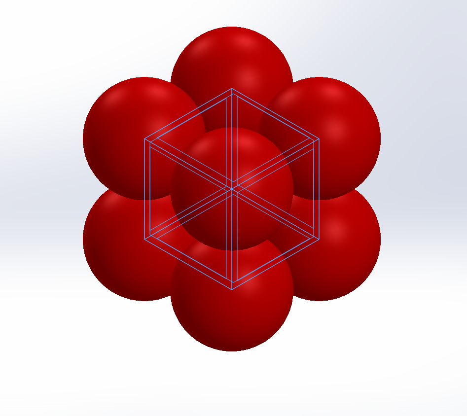
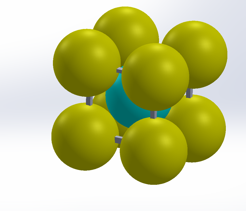
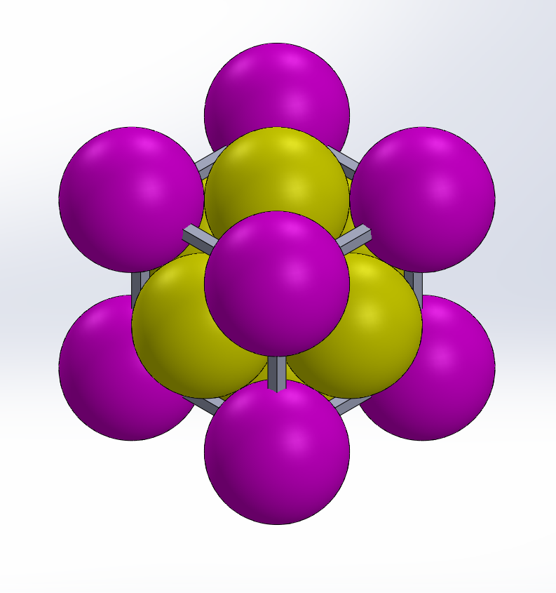
The three cubic unit cells (left to right): simple cubic — atoms only at the 8 corners (net 1 atom per cell); body-centred cubic (BCC) — corners plus 1 atom at the body centre (net 2 atoms); face-centred cubic (FCC) — corners plus 1 atom at each of the 6 face centres (net 4 atoms). Images: Elnaz.gharehdaghi, CC0, via Wikimedia Commons.
Packing and Radius Ratio
- Hexagonal close packing (hcp) and cubic close packing (ccp) both achieve 74% efficiency
- Radius ratio r/R predicts coordination number in ionic solids: 0.155–0.225 → 3; 0.225–0.414 → 4 (tetrahedral); 0.414–0.732 → 6 (octahedral); 0.732–1.000 → 8 (cubic)
Point Defects
- Schottky defect: Equal numbers of cations and anions missing; reduces density; common in NaCl, KCl
- Frenkel defect: Ion displaced from its site to an interstitial position; no change in density; common in AgCl, ZnS
- Metal excess defect: Extra cations in interstitial sites with electrons to maintain neutrality; makes solid n-type semiconductor; e.g., ZnO on heating
- Metal deficiency defect: Fewer cations; some higher-valence cations balance charge; makes solid p-type; e.g., FeO, FeS
Electrical Properties and Band Theory
- Conductors: overlapping valence and conduction bands
- Insulators: large energy gap between valence and conduction bands (>3 eV)
- Semiconductors: small energy gap (~1 eV); conductivity increases with temperature
- n-type semiconductor: doped with higher-valence element (e.g., P in Si); extra electrons carry current
- p-type semiconductor: doped with lower-valence element (e.g., B in Si); holes carry current
Magnetic Properties
- Diamagnetic: All electrons paired; repelled by magnetic field; e.g., NaCl, TiO₂
- Paramagnetic: Unpaired electrons; weakly attracted; e.g., O₂, Cu²⁺ salts
- Ferromagnetic: Unpaired electrons align parallel in domains; strongly attracted; permanent magnets; e.g., Fe, Co, Ni
- Antiferromagnetic: Adjacent spins align antiparallel; net magnetic moment zero; e.g., MnO
- Ferrimagnetic: Unequal antiparallel spins; net magnetic moment present; e.g., Fe₃O₄
Quick Tips
- Number of atoms in a unit cell: corner atom = 1/8; face atom = 1/2; body atom = 1; edge atom = 1/4
- For BCC: 4r = a√3; for FCC: 4r = a√2
- Packing efficiency = (volume of atoms in unit cell / volume of unit cell) × 100
🚀 JEE Advanced Edge
Density from unit cell data: ρ = (Z × M)/(NA × a³), where Z = number of atoms/formula units per unit cell, M = molar mass, NA = Avogadro's number, a = edge length. This is the standard formula linking crystallography to a measurable bulk property, and a very common JEE numerical.
Distinguishing Schottky vs Frenkel by density: Schottky defects (missing ion pairs) measurably DECREASE the crystal's density since mass is lost without volume changing; Frenkel defects (ion just moved to an interstitial site) cause NO change in density since no mass leaves the crystal — this is the key experimental distinguishing test.
Worked problem: A metal crystallises in FCC structure with edge length 400 pm and density 8.95 g/cm³. Find its molar mass. Approach: Z=4 for FCC. ρ = ZM/(NA·a³) → M = ρ·NA·a³/Z = (8.95 × 6.022×10²³ × (4×10⁻⁸)³)/4 = (8.95 × 6.022×10²³ × 6.4×10⁻²³)/4 ≈ 86.4 g/mol (close to Rb, illustrating the calculation method even if the exact element varies by rounding).